


Correlative Analytical Workflow with STEM-CL and EDS for Photovoltaic and Optoelectronic Devices
Cathodoluminescence (CL) spectroscopy in the scanning transmission electron microscope (STEM) enables direct nanoscale mapping of band gaps and defect-induced sub-band-gap states, providing unique insight into the optoelectronic properties of photovoltaic and optoelectronic devices.
In this webinar we present a correlative microscopy workflow that combines SEM-CL, FIB-SEM and STEM-CL. Using CdTe-based photovoltaic thin films and InGaN-on-Si LEDs, we will discuss practical considerations for optimizing STEM-CL experiments, including FIB specimen preparation with a range of ion species, the influence of specimen thickness, and the role of cryogenic cooling in maximising CL signal quality and spatial resolution.
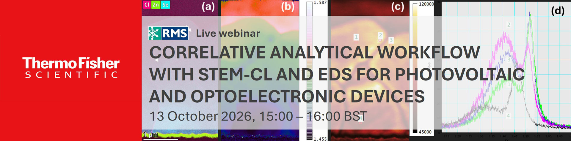
We will demonstrate how STEM-CL analysis delivers nanoscale band-gap mapping, complementary to HAADF imaging and EDS, revealing how defects and alloying elements influence local band-gap variations and device performance.
The webinar will also introduce the instrumentation used throughout the workflow, including a Thermo Fisher Scientific Xenon Helios G4 plasma FIB equipped with a Gatan Monarc-Pro CL system for SEM-CL and TEM lamella preparation, and a Talos F200i STEM fitted with an Attolight Mönch CL detector and a Mel-Build liquid-nitrogen holder for STEM-CL measurements.